Research Interests
Physics of Layered Device Materials
Layered materials have great technological importance: they are often use to store hydrogen, as proton conductors, or as battery electrodes. However, in a lot of cases precise knowledge of the mechanisms of the functionality of these materials is lacking. Such knowledge is nevertheless crucial to achieve optimal material performance. Experimentally it is often extremely difficult to obtain atomistic details of the material processes while the material is operating, e.g., when a battery is charging or discharging. Unintentional defects or intentional doping can influence device performance dramatically. First-principles calculations can pinpoint the atomistic details of the material performance, e.g., the ionic and electronic transport properties, and elucidate the role of defects and impurities. A lot of these materials contain transition metals, so often electronic transport is mediated by polarons, which are localized charges combined with a distortion of the lattice.
Novel Photovoltaic Materials
Solar energy is a very abundant and clean source of energy, which has the potential to provide a significant amount of the world's projected energy needs. However, in order to realize this potential, the performance of the solar cells has to be increased, while at the same time decreasing their costs. Achieving this ambitious goal requires the development of new materials and new device concepts. Highly accurate first-principles calculations can be used to investigate promising new materials and guide experimental efforts.
Material Properties in Lower Dimensions
At lower dimensions, the atomic and electronic structure of materials can change dramatically. For example, quantum confinement effects can occur (but not always, see, e.g., my work on mono-and multilayer MoS2 and nanolayers of Ga2O3), which increase the band gap, and thus modify the absorption spectrum. At the same time, excitons are also quantum confined, increasing their binding energy, and modifying the absorption spectra.
Another important phenomenon that occurs for lower dimensional systems is the so-called dielectric confinement. This effect is caused by abrupt changes in the dielectric constant inside and outside of the material. In classical electrostatics this can be described easily by solving the Poisson equation. However, a similar effect occurs for quantum-mechanical systems, but it is typically not treated with standard DFT methodologies. It is important to include in nanowires, but it is unclear how important this effect is in other low-dimensional systems.
Research Highlights
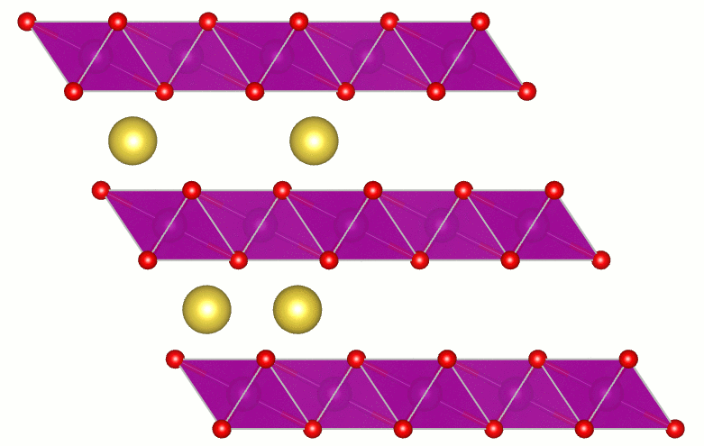
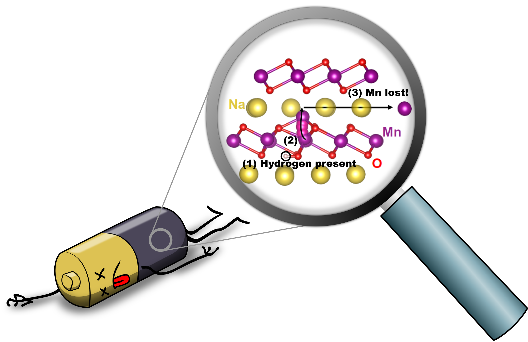
Hydrogen-Induced Degradation of Battery Cathodes
Batteries power our lives: we rely on them to keep our cell phones and laptops buzzing and our hybrid and electric cars on the road. Ever more widespread adoption of the most commonly used lithium-ion batteries may actually lead to increased cost and potential shortages of lithium—which is why sodium-ion batteries are being intensely researched. Their performance is good, and sodium is cheap and abundant; however, the sodium-ion batteries have shorter lifetimes than their lithium-based siblings. Our research revealed the presence of hydrogen as the culprit. Read more details at phys.org, sciencedaily, The UCSB Current, and several other locations.
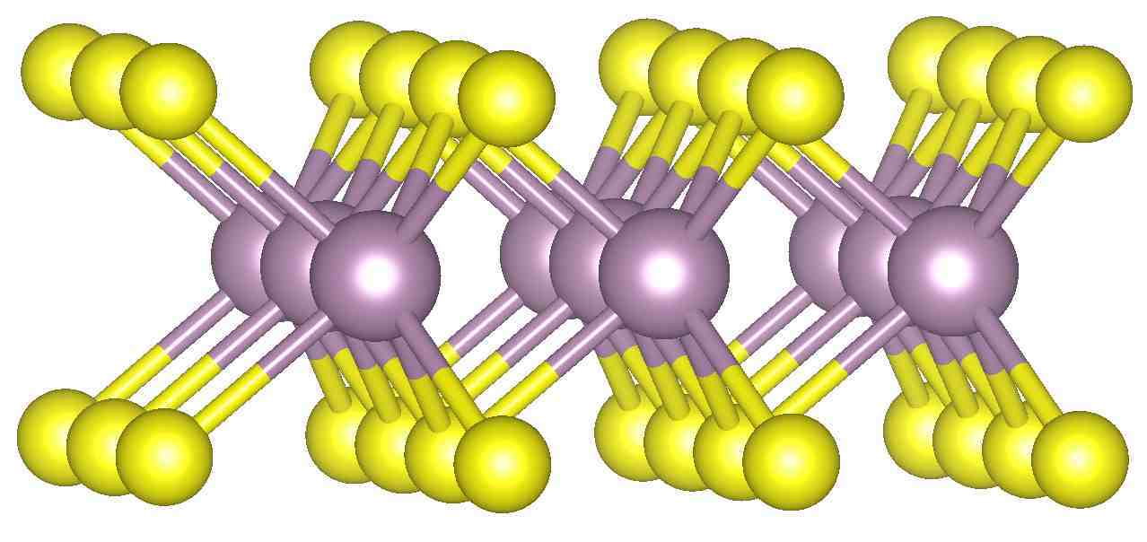
Transparent Conducting Oxides
Transparent conducting oxides (TCOs) are a technologically important class of materials with applications ranging from solar cells, displays, smart windows, and touch screens to light-emitting diodes. TCOs combine high conductivity with transparency in the visible region of the spectrum. A fundamental understanding of the factors that limit transparency in TCOs is essential for further progress in materials and applications. Direct transitions do not lead to absorption of visible light. However, indirect processes, such as those mediated by phonons, can lead to absorption. Using calculations I showed the size and nature of the fundamental limit of the transparency of SnO2. This important result received wide spread attention: by the editors of Applied Physics Letters (selected as a research highlight and as Editor's Pick for the journal's 50th Anniversary), by the scientific community (7th most read article in January 2013), by the scientific blogosphere (e.g., physorg.com, photonics.com, sciencedaily.com,...), by the trade press (Photonics Spectra), and by the regular press (Santa Barbara News-Press).
Artist’s impression of key results. Three beams of light (red for infrared, yellow for visible light, and violet for ultraviolet) travel through a layer of SnO2. Absorption by the conduction electrons in the oxide reduces the intensity of the beams. The calculations showed that absorption is 5 times stronger for ultraviolet and 20 times stronger for infrared, compared to absorption of visible light. There is no sound in this video. |
Layered Materials
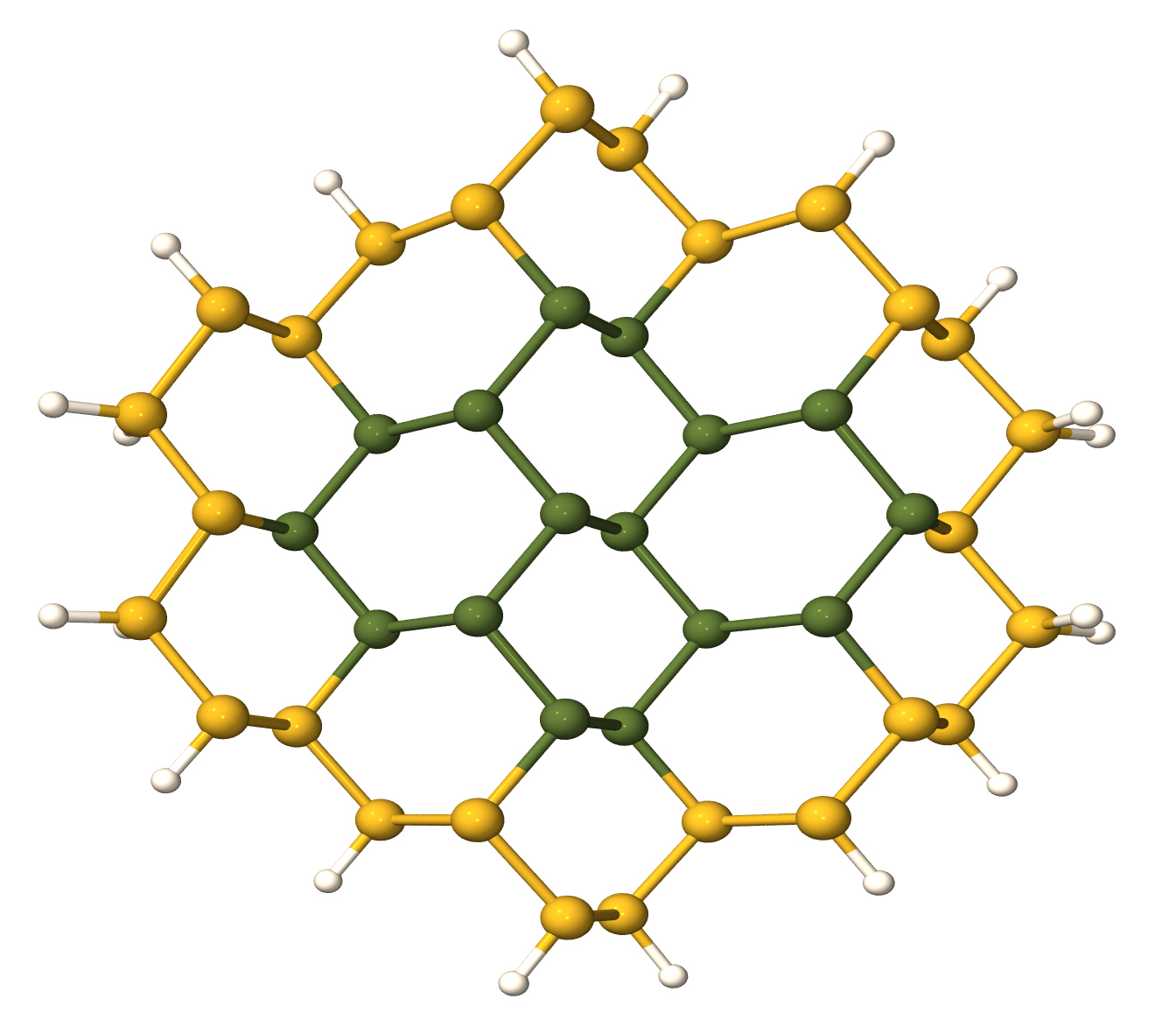
Layered materials show a lot of promise as materials for a wide range of devices, as evidenced by the 2010 Nobel Prize in Physics awarded for graphene, a single layer of carbon atoms. However, graphene lacks a band gap, hindering effective device applications. One possible approach I studied to open a gap is by bonding fluorine atoms to a graphene layer, called fluorographene. Other two-dimensional materials are also highly promising. Recent experiments on molybdenum disulfide (MoS2) showed that it could be used in FETs. However, a lot of crucial information about the band structure and electronic properties of this material is still lacking, hampering interpretation of experiments and preventing accurate device modeling. I have therefore calculated key materials parameters such as band gaps and effective masses, as well as performed an investigation of the effects of strain. I showed how strain allows engineering the nature (direct vs indirect) and size of the band gap and the magnitude of effective masses. In addition, insight into the fundamental physics was obtained by considering the transition between the bulk and the monolayer. This work was featured on the National Institute of Computational Sciences (NICS) website.
Semiconducting Nanowires
Nanotechnology is becoming increasingly important for future applications. Nanowires form a possible nanoscale building block and applications in electronics have already been demonstrated, e.g. for field-effect transistors (FET). FETs are building blocks of the semiconductor industry, and it was shown that nanowires have device properties that can exceed the performance of the current technology. Another promising field is the use as sensors for biological and chemical substances; applications as highly sensitive sensors for virus particles and cancer markers have already been shown. Control of dopant incorporation is essential for these applications. I have performed detailed studies, using a variety of computational techniques, of boron and phosphorus dopants in silicon and germanium, and silicon/germanium core-shell nanowires. The results have allowed me to explain the experimentally observed conductance difference between B-doped and P-doped nanowires, and I have predicted that P dopants tend to segregate to the surface of the nanowires, a finding that has been confirmed experimentally.